10 Subwoofer,8 Ohm Woofer,Best Subwoofer,Subwoofer Bass Ningbo Sonice Electroacoustic Science and Technology Co., Ltd. , https://www.secspk.com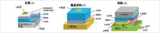
What is an LED flip chip? In recent years, in the field of chips, flip-chip technology is emerging, especially in the market for high-power, outdoor lighting applications. However, due to the late development, many people do not know what is called LED flip chip. What are the advantages of LED flip chip? First of all, from the LED dressing chip to explain the LED flip chip, and the advantages and popularization of LED flip chip.
What is LED dressing chip
The LED package chip is an early chip structure and a chip structure commonly used in small power chips. In this structure, the electrode is on top, and the material from top to bottom is: P-GaN, light-emitting layer, N-GaN, substrate. Therefore, it is a formal dress compared to flip-chip.
LED flip chip and symptom chip diagram
In order to avoid the LEDs occupying the light-emitting area in the pre-loaded chip and affecting the luminous efficiency, the chip developer designed the flip-chip structure, that is, the flip-chip is inverted, so that the light excited by the light-emitting layer is directly emitted from the other side of the electrode (the substrate is finally stripped). The chip material is transparent. At the same time, the structure of the LED package factory wire bond is designed for the flip chip. Therefore, the whole chip is called a flip chip, and the structure is widely used in high power chips.
Three major genres of dressing, flip-chip, vertical LED chip structure
Flip-chip technology is not a new technology, but it existed long ago. Flip-chip technology is not only used in the LED industry, but also in other semiconductor industries. At present, LED chip packaging technology has formed several genres, and different technologies have different characteristics for different applications.
At present, there are three main types of LED chip structures, and the common ones are formal structures, vertical structures and flip-chip structures. The positive-fit structure is prone to current crowding due to the p and n electrodes on the same side of the LED, and the thermal resistance is high, while the vertical structure can solve these two problems well, and can achieve high current density and uniformity.
In addition to the material cost, the reduction of the cost of the future lamps is particularly important in reducing the number of LEDs. The vertical structure can well meet such requirements. This also results in vertical structures typically used in high power LED applications, while formal technology is typically used in small and medium power LEDs.
Flip-chip technology can also be subdivided into two categories, one is flip-chip based on sapphire chip, the sapphire substrate is reserved for heat dissipation, but the current density is not obvious; the other is flip-chip structure and stripped The bottom material can greatly increase the current density.
What is LED flip chip
The reason why flip chip is called "flip-chip" is compared to the traditional wire bonding method (Wire Bonding) and the post-bulb process. Conventionally, the electronic surface of the wafer connected to the substrate by metal wire bonding is facing upward, and the electrical surface of the flip chip is facing downward, which is equivalent to turning the former over, so it is called "flip chip".
The LED chip is flip-chip mounted, and a GaN-based LED structure layer is grown on the sapphire substrate by MOCVD technology, and light emitted from the P/N junction light-emitting region is emitted through the upper P-type region. Due to the poor conductivity of P-type GaN, in order to obtain good current expansion, a metal electrode layer composed of Ni-A is formed on the surface of the P region by evaporation. The lead of the P region is taken up through the metal film of the layer.
To achieve good current spreading, the Ni-Au metal electrode layer should not be too thin. For this reason, the luminous efficiency of the device is greatly affected, and it is usually necessary to take into account both the current expansion and the light extraction efficiency. However, in any case, the presence of the metal film always deteriorates the light transmission performance. In addition, the presence of wire bonds also affects the light extraction efficiency of the device. The structure using GaN LED flip chip can fundamentally eliminate the above problems.
Based on the technology of flip chip, LED flip chip gold-free chip scale package has been developed.
What is LED flip-chip gold-free chip scale package
Flip-chip gold-free chip-scale package, based on flip-chip soldering technology, on the basis of traditional LED chip packaging, reduce the gold wire packaging process, save the lead frame, wire, leaving only the chip with phosphor and package adhesive . As a new packaging technology product, the flip-chip gold-free chip-level light source has no problems such as no light, flicker, and high light decay caused by gold wire soldering or poor contact. Compared with the traditional packaging process, the package density of the chip-scale light source has increased by 16 times, the package size has been reduced by 80%, and the luminaire design space is larger.
The flip-chip gold-free chip is favored by more and more LED lighting companies and terminal product application companies with more stable performance, better heat dissipation, more uniform light color distribution and smaller volume.
Difficulties in the popularity of LED flip chip
Flip-chip LED technology currently has greater advantages in high-power products and integrated packaging. In small and medium-power applications, cost competitiveness is not very strong.
From the chip to the package, this will require higher equipment. Take the package and say that the cost of the front-end equipment that can be flip-chip will definitely increase a lot. This sets the threshold, so that some enterprises can not access this technology. .